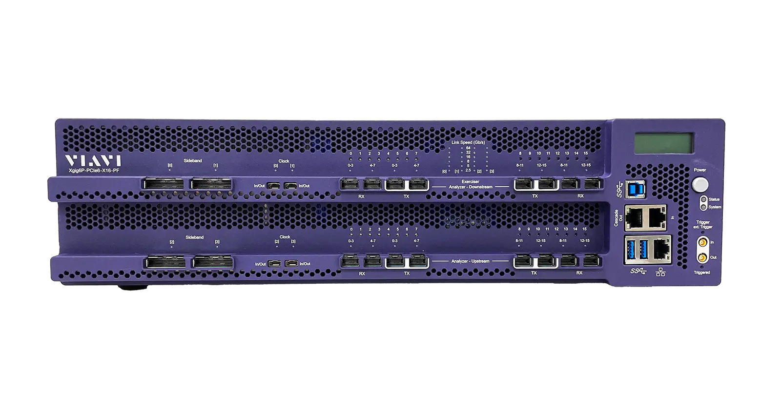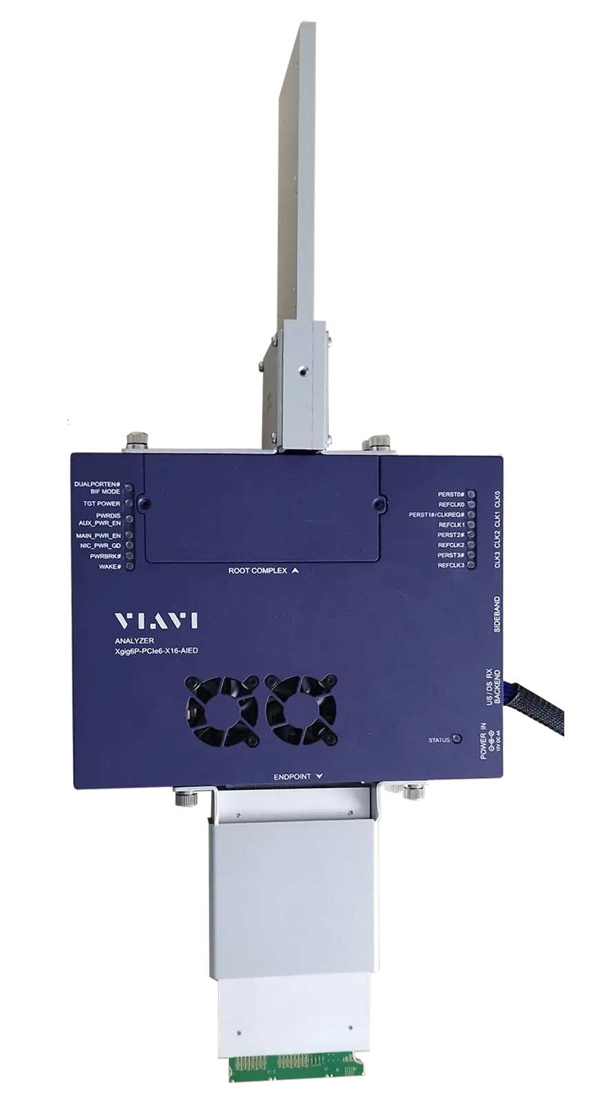
Xgig XGIG6P-PCIE6-X8-IE3 PCIe 6.0 x8 Analyzer/Exerciser Front End EDSFF E3
PCIe 6.0 x8 Analyzer/Exerciser front end for EDSFF E3 modules, used with the VIAVI Xgig EDSFF interposer.
- Maximum data rate
- 64GT/s PCIe 6.0
- Supported PCIe data rates
- 2.5, 5.0, 8.0, 16 and 32GT/s
- Supported module form factors (family)
- E1.S, E1.L, E2, E3.S, E3.L, and OCP NIC 3.0
Overview
The VIAVI Xgig EDSFF Analyzer Interposers connect the VIAVI PCIe 6.0 Analyzer/Exerciser chassis to a system under test for up to 64GT/s x16 capture. The Analyzer Interposer installs into an EDSFF slot and provides a fully analog signal path between the root complex and the endpoint, tapping the data signals between host and endpoint devices as input to the Analyzer/Exerciser chassis. It operates at the 64GT/s PCIe 6.0 rate across 16 bi-directional lanes. Variants are available for x16, x8 and x4 lane widths, with mechanical support for E1.S, E1.L, E2, E3.S, E3.L and OCP NIC 3.0 modules.
The interposer uses high-speed linear signal redrivers to buffer system data signals between the slot and the PCB fingers, so that a clean signal reaches both the Analyzer/Exerciser chassis and the DUT for protocol capture and analysis.
Setup
The interposer is inserted into an E1, E2, E3 or OCP NIC 3.0 slot in the host system, and an EDSFF DUT carrier is installed into the interposer to create the test data path. Cables connect the interposer to the VIAVI Protocol Analyzer/Exerciser chassis, which captures tapped DUT data from both the upstream and downstream signal paths. The interposer requires an open DUT system chassis while in use. The XGIG6P-PCIE6-X8-IE3 is one of the ordering items in this interposer family.
Applications
Together with the VIAVI PCIe 6.0 Analyzer/Exerciser chassis, the interposer supports debug and verification of new ICs, new system hardware designs and FPGA firmware, validation of system BIOS and software, and manufacturing test.
Key Features
- Operates at 64GT/s PCIe 6.0 data rates
- Supports 2.5, 5.0, 8.0, 16 and 32GT/s PCIe data rates
- Fully analog signal path between root complex and endpoint
- High-speed linear signal redrivers buffer system data signals
- 16-lane EDSFF 4C/4C+ or 2C slot receptacle accepts all EDSFF endpoint DUT modules
- 16-lane 4C/4C+/2C/1C PCB finger connector installs into the host test system's EDSFF slot
- Supplied with custom data cables for signal capture with minimal tuning effort
- Analyzer Interposer power is independent of the host system
- Front End Attachments can rotate 90 degrees for positioning
Specifications
| Maximum data rate | 64GT/s PCIe 6.0 |
|---|---|
| Supported PCIe data rates | 2.5, 5.0, 8.0, 16 and 32GT/s |
| Supported module form factors (family) |
E1.S, E1.L, E2, E3.S, E3.L, and OCP NIC 3.0
Across the interposer family
|
| Assembly | Analyzer/Exerciser Front End |
|---|---|
| Lane width | x8 |
| Form factor | EDSFF E3 |
Specifications are taken from the manufacturer's documentation. See the datasheet for complete and current values.
Applications
- Debug and verification of new ICs
- New system hardware design verification
- FPGA firmware debug
- System BIOS and software validation
- Manufacturing test
- PCIe 6.0 protocol capture and analysis
Included
- Cables, cords, brackets and instructions necessary for proper operation (contents vary by selected product)
Options & Accessories
| Option | Description |
|---|---|
| XGIG-INTPSR-C-Hx | x-year extended hardware warranty — x=1,2,3,4 |
| XGIG6P-PCIE6-AIE3 | E3.X DUT Carrier |